 Fraunhofer Institute for Microstructure of Materials and Systems IMWS
Power semiconductors made of gallium nitride increase energy efficiency and save resources
In the EU-funded project "Ultimate GaN", 26 partners from nine European countries conducted joint research on the next generation of gallium nitride (GaN)-based power semiconductors. The consortium of industry and research partners developed compact, cost- and energy-efficient components based on gallium nitride, which open up new possibilities especially in the fields of smart mobility, smart grids and 5G communication.
Digitalisation in industry and private households, the expansion of electromobility as well as the growing demand for sustainable and affordable energy and the necessary reduction of CO2 emissions are currently dominant topics. Meeting these challenges requires the efficient generation, control and use of energy. Within this context power semiconductors that control and switch high electrical currents and voltages play an important role. Conventional silicon-based semiconductors are reaching their limits and are increasingly being replaced by GaN semiconductors. These offer more performance in a smaller space, save energy and thus minimise the carbon footprint.
However, the special chemical-physical material properties of GaN wide-band-gap semiconductors and the structure of high-electron mobility transistors raise new questions: "The high electric field strengths and enormous current and power densities with correspondingly high material stress in these very compact components pose particular challenges.", says Frank Altmann, Head of the Business Unit "Materials and Components for Electronics" at the Fraunhofer IMWS.
In the recently completed research project "Ultimate GaN", a consortium of 26 European partners from science and industry under the leadership of Infineon Austria set themselves the task of harnessing the advantages of GaN technology along the entire value chain, from process development, design, assembly and interconnection technologies to integrated system solutions.
With high-resolution analysis procedures and innovative fault diagnosis methods the Fraunhofer Institute for Microstructure of Materials and Systems IMWS contributed to process optimisation and increasing the reliability of the GaN devices."We are researching specific critical defects or GaN-specific degradation processes in order to be able to detect, understand and thus avoid new failure modes as early as possible," says Frank Altmann.
For example, leakage current paths were localised after reliability testing and investigated microstructurally to determine their cause. As such, a new defect signature was identified that led to the premature electrical breakdown of special semi-vertical GaN transistors. On the basis of these findings, the manufacturing process could be systematically optimised.
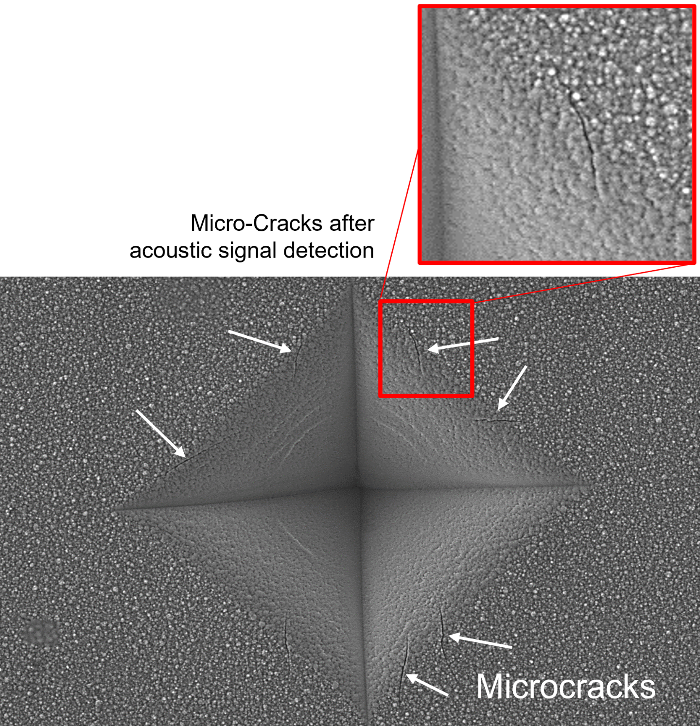
With nanoindentation testing in combination with acoustic emission, IMWS scientists were able to detect hidden microcracks under the metallisation layers of bond pads. The above mentioned methodology was applied and evaluated on different processed samples of the project partners and the related defect structures were investigated by electron microscopy analyses.
The European project "UltimateGaN" (Research for GaN technologies, devices and applications to address the challenges of the future GaN roadmap) had a duration of three and a half years. The project volume of 48 million euros was financed by investments from industry, grants from the individual participating countries and the European “Joint Undertaking” ECSEL (Electronic Components and Systems for European Leadership).
![Image 1 in printable resolution. The illustration may be used free of charge for editorial purposes for reporting on this topic. Use for other purposes is only permitted with the prior consent of the Fraunhofer IMWS. [ PNG 7.04 MB ]](/content/dam/imws/de/images/Kompetenzfelder/Mikroelektronik/11_GF2_Leistungshalbleiter%20(004).png)
![Image 2 in printable resolution. The illustration may be used free of charge for editorial purposes for reporting on this topic. Use for other purposes is only permitted with the prior consent of the Fraunhofer IMWS. [ PNG 3.78 MB ]](/content/dam/imws/de/images/Kompetenzfelder/Mikroelektronik/11_GF2_Leistungshalbleiter.png)