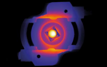
Despite their high efficiency, an LED reaches very high thermal power densities during use. Thus, for electrical power 1 W and 90 percent efficiency, the heat output per unit area is 100 kW/m². This is roughly twice that of a standard hot plate. On the one hand, high operating temperatures have a negative effect on the life of the LED (the life reduces exponentially with increasing temperature), on the other hand they cause unwanted LED color change in the long term.
Non-contact and spatially resolved determination of the surface temperature of LED modules is possible with the help of infrared thermography. In this way it is possible to identify the areas of the component subject to higher thermal stress. The interesting areas to be examined are often not on the surface, but are covered by other materials such as encapsulation materials or caps, which are only partially transparent to infrared. Fourier transform infrared spectrometry, with which the effect of various materials on thermographic measurement can be determined, is used to characterize the transmission of these materials within the infrared structural range. Even higher spatial resolution is required to map hotspots within an LED package. At the Fraunhofer AWZ we have an infrared microscope that enables resolutions within the range of a few micrometres, which can be used for these measurement tasks.
The heat capacity, the thermal conductivity and the geometry of the materials and assemblies involved must be known in order to describe the heat transport within an element. Calorimetric and microscopic methods of measurement are available for this. The investigation results can be used to reconsider the composition of the components and adjust them effectively to increase their efficiency and life.
