The coating of modern microelectronic components requires the lowest possible process temperatures. PSC GmbH would like to offer pentachlorodisilane (PCDS) as an efficient, innovative starting material for this demanding process. At the Fraunhofer Center for Silicon Photovoltaics CSP, new methods of ultratrace analysis are being developed in parallel to ensure that the manufacturing processes meet the highest quality requirements.


Materials are frequently coated in order to make them even more efficient for use in various everyday products: This makes mobile phone displays scratch-resistant, saw blades even harder, and window panes are given a heat protection layer. High-quality microelectronic components such as computer chips or sensors are also coated. The layers applied to the actual material can serve, for example, as insulation between various components or can later be etched into them as “tunnels” and “channels” that serve as conductor paths.
The process of chemical deposition is particularly attractive for the coating of microelectronic components. This process allows even complex surfaces to be coated well and uniformly, which is exactly what modern chips need because they have very filigree, three-dimensional architectures within a very confined space. The principle of chemical deposition is that gaseous starting materials (precursors) are guided over a substrate and thereby chemically decomposed (for example by heating or excitation with light or a plasma), resulting in a new layer being deposited as a solid on the substrate surface.
The precursors required for this are the main product of PSC GmbH in Bitterfeld-Wolfen. Besides applications in the solar industry (production of polysilicon), disilanes are used especially frequently for the most advanced technological stages in microelectronics (i.e. the smallest structure widths) as starting material for the most diverse deposition processes. This is the only way to achieve the particularly low process temperatures that are essential for highly integrated chips: In such components, individual layers are often only a few nanometers wide, which is why they do not tolerate high temperatures in the manufacturing process. Disilanes as precursors make low process temperatures possible, with hexachlorodisilane (Si2Cl6, HCDS) in particularly high demand.
Together with the Fraunhofer CSP, PSC GmbH aims to develop new precursors that make even lower deposition temperatures possible. These are necessary for the requirements of the next generations of microelectronics technology. The company has already identified pentachlorodisilane (HSi2Cl5, PCDS) as a material with good prospects. Substituting a chlorine atom for a hydrogen atom makes the molecule thermally more unstable than HCDS, which means that deposition can take place at even lower temperatures. So far, PSC GmbH is the only company able to offer this precursor, but only in technical quality and on a laboratory scale (gram quantities). Together with the Fraunhofer team, they aim to find a way to produce high-purity PCDS in large quantities. Besides the actual manufacturing process, which is being developed by PSC GmbH, this also requires new analytical methods, which are to be developed in the joint project at the Fraunhofer CSP which will run until October 31, 2021.
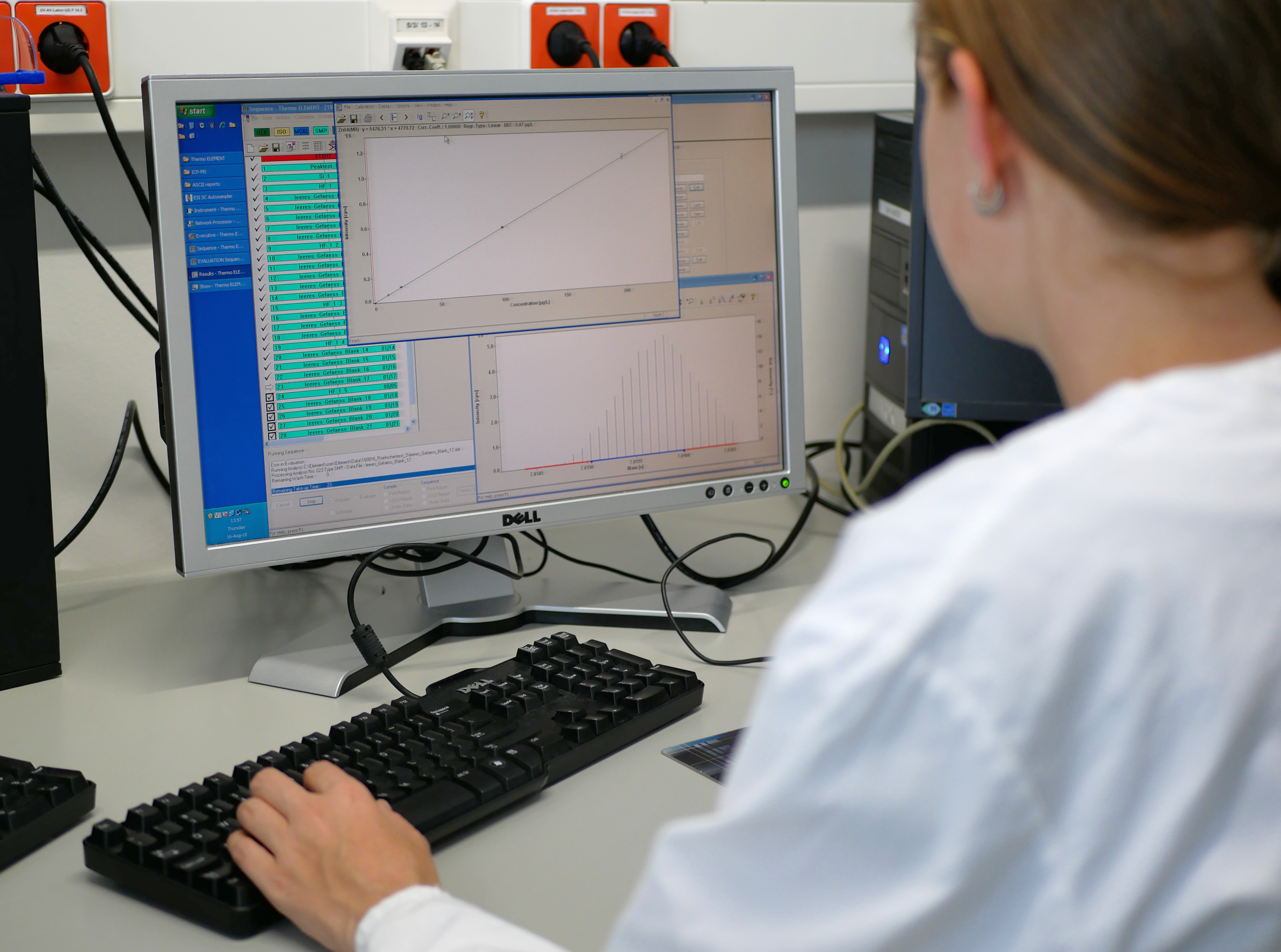
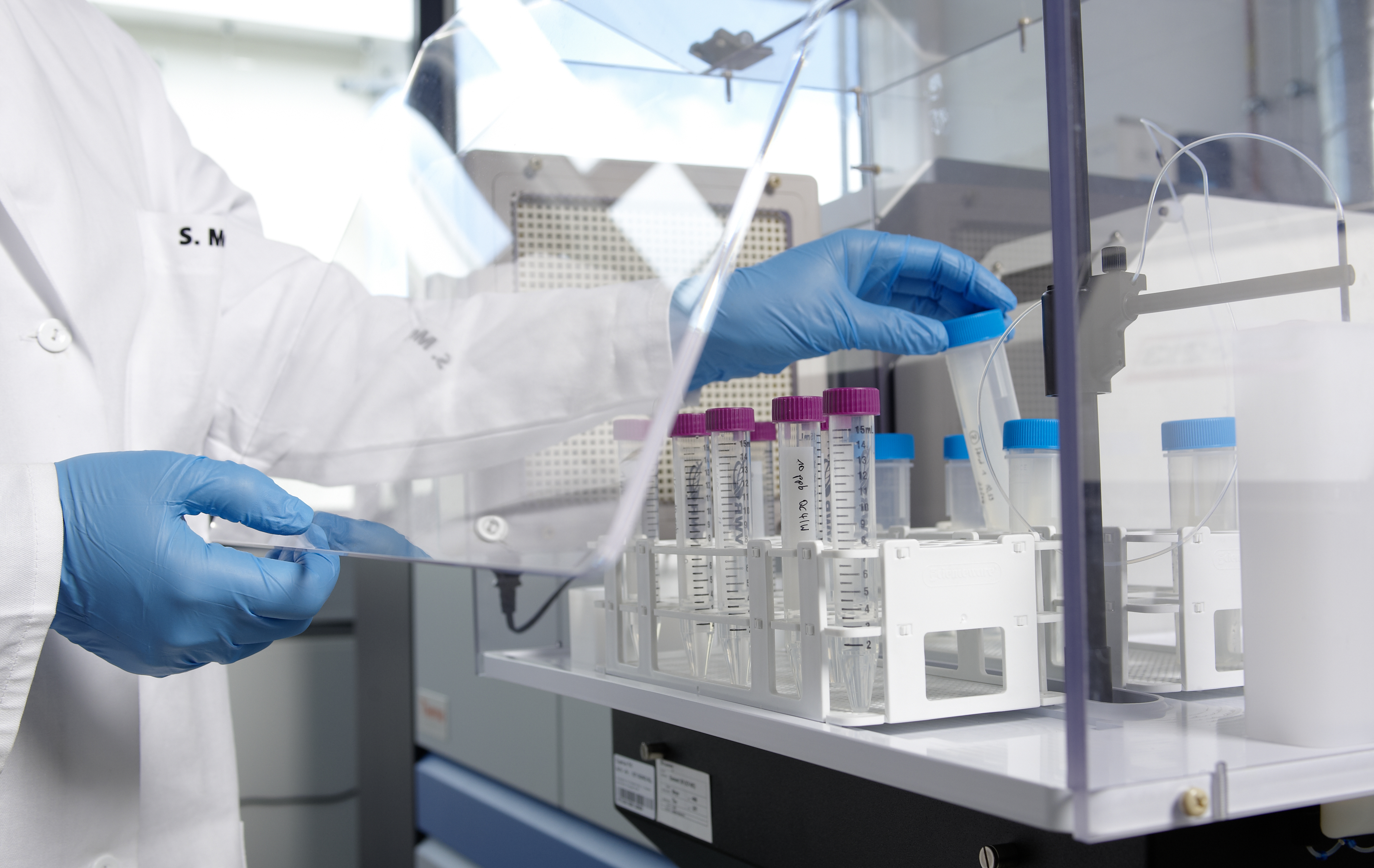
“To ensure that new microelectronic materials are stable during production and reliable later in use, ultra-high purity qualities are required. This means that contamination is only permitted in the low single-digit parts-per-billion range. Otherwise, metallic elements, for example, can damage the circuits. To prevent this, we want to develop a suitable, reliable and routine method for ultratrace analysis,” says Dr. Sylke Meyer, Head of the “Materials and Processes” Group at the Fraunhofer CSP, which is overseeing the project. The Fraunhofer CSP is contributing its extensive expertise in the ultratrace analysis of silicon. Moreover, excellent equipment for sensitive elemental analysis is available for the project.
The new ultratrace analysis methods would then be applicable not only for PCDS, but also for other starting materials in coating processes. After all, customer requirements for the purity of the product are constantly increasing even with HCDS, the most powerful precursor material to date. Last but not least, the new methods can also support the development of further products of the next generation of precursors based on longer-chain oligochlorosilanes, which are promising key materials for future markets in printable electronics as well as for a large number of high-performance ceramic applications.
“One particular challenge is to design the work steps during the analysis in such a way that no additional impurities are introduced. We have already completed the first successful preliminary tests, so I’m confident that we can achieve this. The new analytical method has a high market potential. The same applies to PCDS as a new, powerful precursor for the semiconductor market,” says Meyer.