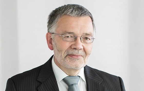
Together with partners in industry, the Fraunhofer IMWS not only works on the diagnostics of materials and the tailormade development of new materials. It also develops new equipment for microstructure elucidation together with its clients. In the interview, Prof. Dr. Matthias Petzold, Head of the »Center for Applied Microstructure Diagnostics CAM« business unit, explains the advantage this offers.
You work closely together with equipment manufacturers. What do these companies want to achieve in their collaboration with the Fraunhofer IMWS?
They are faced with the task of keeping up, or even being a step ahead, of the very fast advances in the development of new, more efficient materials or in microelectronics technologies. We offer them three things: joint development of new techniques, application support for a fast market launch and manifold potential customer contacts.
What do you mean by manifold contacts?
Within the scope of our cooperation projects with industrial technology leaders, for example, from the electronics industry or the manufacture of innovative functional materials, we also try to involve our partners in the field of diagnostics instrument engineering in the development of new products at an early stage. This enables them to carry our preliminary research for potential clients, which is tailored to their requirements. In this way they can acquire a head-start by working on special customized analysis solutions in advance of future production, which are then required later for technology qualification and quality assurance in production. At the same time, through this collaboration, additional contacts to future users of the new instrument technology emerge. We naturally also accept test and diagnostics enquiries from users and work up innovative solutions together with the instrument manufacturers. Apart from industrial projects, to this end we also cooperate in large European collaborative projects. In the field of microelectronics, some of these projects include up to 40 partners from different countries, whereby the diagnostics and test suppliers work together with the leading European research institutes and semiconductor technology companies. Last but not least, the developments achieved through a large research project also become known more quickly, which makes companies curious.
Can you name a few examples of instrument or equipment developments?
Over recent years we have developed lock-in thermography, a new method for detecting defects in microelectronics by means of highly sensitive thermal imaging. Launched on the market by our industrial partner, the technique was very well accepted internationally and is now used by more than 50 leading major electronics manufacturers worldwide. In addition, we are currently working on a device which is aimed at detecting concealed defects inside electronic components and the evaluation of mechanical film properties by means of ultrasound microscopy within the gigahertz range. Here we are cooperating closely with manufacturers not only in device hardware but also in software development. A third market-ready example is fast, efficient sample preparation methods by means of high-precision laser technologies, which significantly improve the throughput of high-resolution analysis techniques. Our industrial development partner is currently launching the device on the market. But there are many other examples, for example, in the field of mechanical test engineering and testing, and we would like to expand this field still further in the future.
