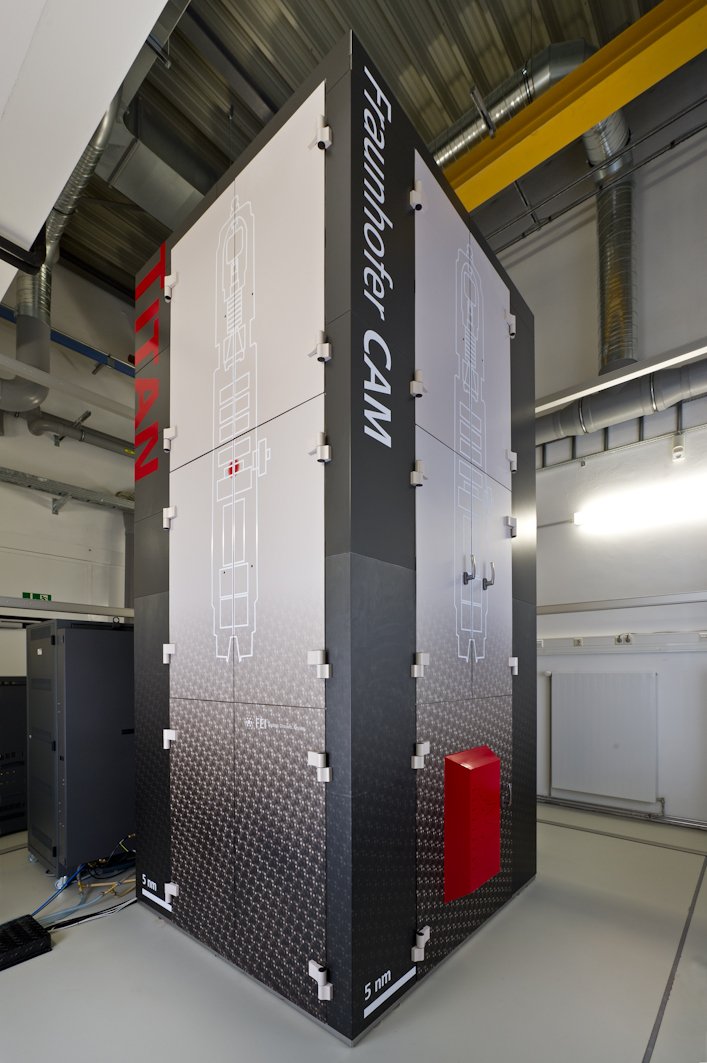
Our clients receive a unique and comprehensive offer for failure analysis and material characterisation. Grouped together in a single centre to save time and costs, run by a committed and service-orientated team, which has excellent knowledge of material-induced problems in microelectronics. In addition there are top level technical facilities - the Fraunhofer IMWS has the most comprehensive equipment for microstructure elucidation within the Fraunhofer community.
Non-destructive defect localisation
- Scanning acoustic microscopy (MHz, GHz)
- Lock-in and pulse-phase thermography
- X-ray analysis and 3D tomography
Target preparation techniques
- Delayering (CMP)
- Metallographic preparation and chemical decapsulation
- Use of laser beams for decapsulation and making transverse sections
- Use of ion beams to make transverse sections and for polishing
- Locally limited mechanical grinding method, preparation from the IC rear
- Cryo ultramicrotome, rotating microtome
Focused ion beam method and electron microscopy
- High-performance FIB system and chem. etching of grooves in Si, integrated IR microscope
- Crossbeam FIB system with EDX and EBSD
- Crossbeam FIB system for the TEM Lift-out method
- ESEM FIB system with cryo transfer
- Low-energy Ar FIB techniques for sample finishing for TEM tests
- Various high-resolution SEM with electrical in-situ contact and EBIC/EBAC
- Analytical SEM with EBSD, EDX, WDX
- Environmental SEM (ESEM) with in-situ investigations and levels
- TEM (200 kV) with ns-EDX and in-situ investigations
- TEM (200 kV) with ns-EDX, EELS, NBD
- EF-TEM (60-300 kV) with Cs correction, EDX, EELS, HAADF, STEM
Surface and trace analysis
- Atomic force microscopy (AFM)
- Photoelectron, UV and auger electron spectroscopy (XPS/UPS, AES)
- Time of flight secondary ion mass spectrometry (TOF-SIMS)
- Mass spectrometry with inductive coupled plasma (ICP-MS)
- Contact angle measurements
Crystallography and optical spectrometry
- Micro X-ray diffraction (XRD)
- Electron backscatter diffraction (EBSD)
- IR, light and fluorescent microscropy
- UV/VIS, fluorescence and FTIR spectroscopy
- Micro-Raman spectroscopy
- Electro / photoluminescence
- IR double refraction investigations (for Si components)
Surface topography and deformation
- Mechanical profilometry
- Laser scanning microscopy
- White light interferometry
- Electronic speckle pattern interferometry (ESPI)
- Image correlation systems for the 3D forming analysis
- Wafer bow and thickness fluctuations
Polymer characterisation
- Dynamic differential scanning calorimetry (DSC)
- Dynamic mechanical analysis (DMA)
- Thermogravimetry (TGA) with FTIR
- Thermomechanical analysis (TMA, dilatometry)
- Thermal conductivity analysis (TCA, laser flash)
- Rheometry
Mechanical testing and evaluation
- Static and dynamic material test machines up into the mN load range
- Nanoindentation (T-dependent) and micro hardness test
- Tension and shear tester for microelectronic interconnection technology
- Individualized MEMS, piezo-driven fatigue tests and wafer contact tests
- MEMS analysis including laser vibrometry, stroboscope video microscopy and white light interferometry
- Electrical test station, parameter analysis
- High throughput, thermal shock, humidity and vibration tests
