 Fraunhofer Institute for Microstructure of Materials and Systems IMWS
Simplification of sample preparation using focused ion beams
Highly integrated microelectronic switches can be found in a large number of modern pioneering technologies. One of the proven methods for the error analysis of such components is the focused ion beam (FIB) technique. A new research project at the Fraunhofer Institute for Microstructure of Materials and Systems IMWS and point electronic GmbH is investigating an innovative approach for nanometer-precise high-throughput sample preparation using FIB with the aim of simplifying the device-dependent methods currently employed.
Autonomous driving, smart home integration and artificial intelligence are just a few examples where microelectronic switches are essential. In order to ensure the functionality and reliability of the components used in such applications, they undergo comprehensive microstructural characterization during the stages of development, manufacture and implementation monitoring. With this in mind for example they are observed and analyzed using transmission electron microscopy (TEM) in order to detect even the smallest defects at scales ranging from ten to a few hundred nanometers.
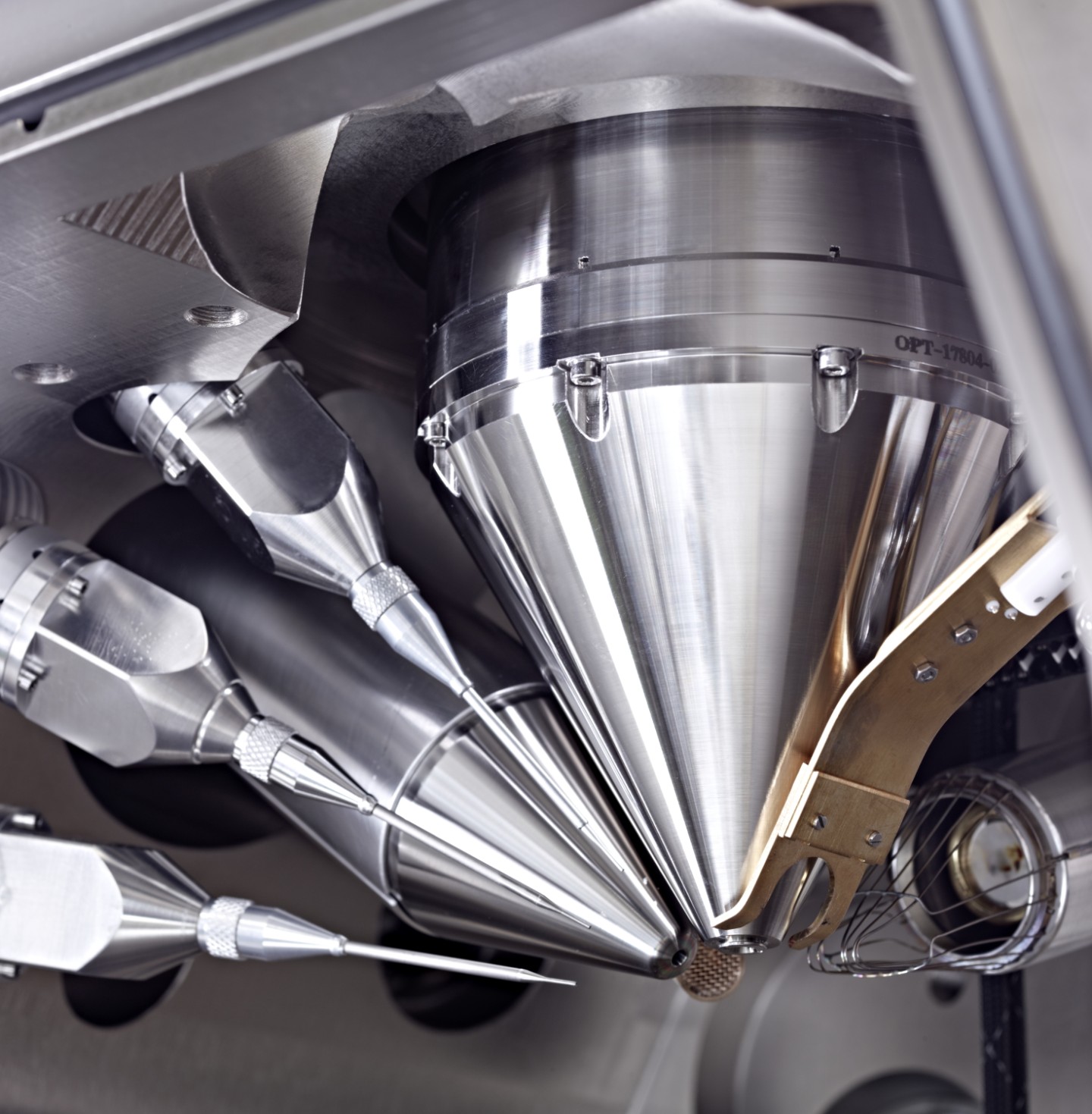
A decisive success factor here is the quality of the samples, which often have to be laboriously prepared using focused ion beams (FIB): the ion beam removes material from the sample until the area due to be examined is thin enough to be studied using TEM. Although the systems employed are characterized by target and process accuracy, they are incapable of simultaneously achieving high precision and a high ablation rate.
“To date it has only been possible to achieve precision through extremely focused and spatially restricted beams, whereas a high ablation rate cannot be achieved using an intensive and hence inevitably less accurate beam”, says Dr. Michael Krause, project manager at the Fraunhofer IMWS, summarizing the problem.
In order to deal with this problem, the Fraunhofer IMWS together with point electronic GmbH is currently investigating a new method for nanometer-precise high-throughput sample preparation using focused ion beams. There are plans to transfer a method already developed for the targeted, local increase in material ablation during the ion beam thinning of flat surfaces to the FIB preparation of TEM samples. The iNotchTM technology developed at the Fraunhofer IMWS provides the basis for this new sample preparation workflow.
point electronic GmbH, with its systems for digital imaging and for controlling electron-optical columns, provides important know-how. These unique conditions will enable the company to develop a special system for controlling the ion-optical columns of FIB systems in the course of the research project scheduled to conclude in spring 2022. If the project partners are successful, the result will be a more powerful method for sample preparation, helping to ensure the reliability of microelectronic components for important emerging technologies.