 Fraunhofer Institute for Microstructure of Materials and Systems IMWS
Detecting security vulnerabilities on the nanoscale
Modern life and advancing digitalization depend crucially on electronic systems. Spectacular cyber attacks in the past have shown the vulnerability of such systems. Advances in the manufacturing technology of nano-electronic components and the increasing complexity of hardware offer a host of further challenges for system security because the focus of attackers has shifted to the hardware level. The Fraunhofer Institute for Microstructure of Materials and Systems (IMWS) is investigating these risks together with the Security in Telecommunications department of the Berlin Institute of Technology (Technische Universität Berlin).

Hardware attacks usually aim to obtain sensitive information. A frequent context here is product piracy: Attackers try to explore the architecture of a chip or the signal processing within an integrated circuit (IC) in order to then be able to copy it.
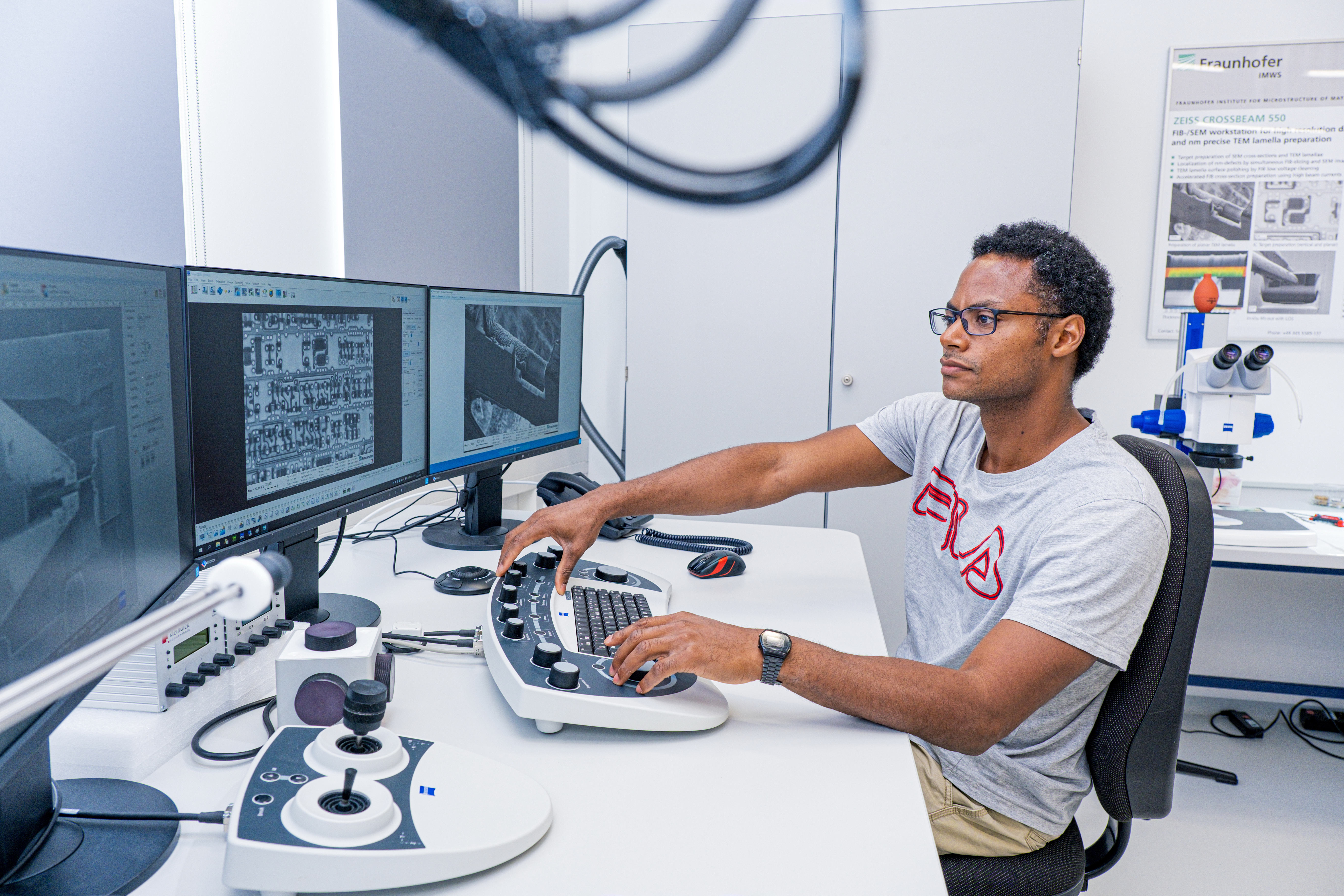
Currently, the most successful attacks on electronic components are optical techniques for IC signal tracking and fault localization. However, due to the miniaturization of technology nodes below 10 nanometers, these methods are reaching their limits. "High-resolution imaging techniques based on scanning electron microscopy offer completely new possibilities here for identifying vulnerabilities and exploiting them for hacker attacks. This is where our project comes in," says Frank Altmann. He heads the three-year project "nanoEBeam" at the Fraunhofer IMWS, which is part of the "Nano Security: From nano electronics to secure systems" funding program of the German Research Foundation (DFG).
"The hackers' approach is somewhat similar to our approach to fault diagnostics: We try to identify weak points in electronic components and determine their causes in order to improve manufacturing processes and ensure high quality and reliability of the components. Hackers look for worthwhile points of attack in a comparable way," Altmann explains. The findings from "nanoEBeam" can therefore not only be used to maintain a knowledge advantage over attackers in the case of new, nano-technological components, but also to further develop fault diagnosis methods such as e-beam probing for the next chip generation.
The project partners are relying on e-beam probing from the back of the chip to gain direct access to the nanoscale transistor level. Compared to optical methods (and the limitations imposed by the wavelengths used in each case), the electron beam offers significantly higher precision for imaging and signal analysis. A major challenge here is to make the remaining silicon substrate of a chip extremely thin without compromising the functionality of the chip. An electron beam then penetrates this thin silicon substrate, and in the scanning electron microscope (SEM), functional structures can thus be recorded and the signal course evaluated for side-channel attacks.
"We must assume that such attack techniques on nano-electronic devices will be feasible in the future, making new attack scenarios possible. During our research work, we will therefore also determine what effort potential attackers have to make and what equipment they need to be able to attack nano-electronic chips. This is the prerequisite for being prepared for such attacks. With our expertise and the excellent equipment of high-resolution diagnostic methods, we can make an important contribution here," says Altmann, summarizing the project goal.