More efficiency of quality checks in the solar industry: New potentials through Raman spectroscopy
In the mass production of solar cells, the purity of the materials used plays a decisive role in the electrical efficiency of the end product. This requires suitable measures for reliable process control. In a joint project, the Fraunhofer Center for Silicon Photovoltaics CSP, the Südwestfalen University of Applied Sciences, Geb. Schmid GmbH and Spectroscopy & Imaging GmbH have opted for a new approach: the aim is for Raman spectroscopy to enable contamination on or in the material to be analyzed by non-destructive and non-contact methods. This could lower production costs while at the same time providing advantages for quality control.
More than 95 percent of the solar cells manufactured worldwide are made of silicon wafers. These are thin slices, which are first cut from large silicon blocks during the manufacturing processes. For example, they can be damaged by the sawing process and also become dirty due to the organic residues from the sawing tool. Such contamination occurs very rarely, but due to the large quantities in the photovoltaic industry, they can nonetheless have a significant effect on total costs. Therefore, time-consuming and expensive processes are necessary to clean the wafers chemically or sort our defective wafers before they are processed further.
»There is no inline-capable method to date that is capable of analyzing such organic residues on wafer surfaces. We want to make Raman spectroscopy usable for this, which at the same time can also check the surface finish directly following the sawing process«, said Prof. Dr. Stefan Schweizer, who heads the project at the Südwestfalen University of Applied Sciences. »If we succeed, we will have an efficient instrument for complete and continuous control of the manufacturing quality in the production of silicon wafers. Possible contamination could be detected early and unnecessary cleaning steps saved. This increases material efficiency, cuts production costs and reduces impact on the environment«, is how he described the objectives.
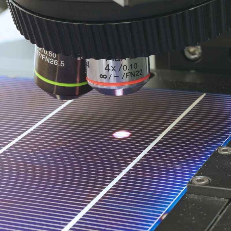
To date, Raman spectroscopy has primarily been used for the analysis of pharmaceutical products and in scientific research. The material to be examined is irradiated by a laser. When the light from the laser source hits the surface of the specimen it is scattered. The distribution of the frequencies in the resulting spectrum can be used to deduce statements about the substance examined and the material properties.
The advantages of Raman spectroscopy compared to other methods: The material does not have to be especially prepared, the checking can therefore be carried out at each step in the process chain without prior specimen preparation. The checking is non-destructive and contactless. In the event of contamination, not only can statements be made about whether a silicon wafer is contaminated, but also how highly and with which substances. Because the backscattered light from different contaminants has characteristic frequencies, the contaminants can thus be identified just like with a fingerprint.
»First we want to determine detection limits, to show that the method has the necessary high detection sensitivity. At the same time, working with the industrial partners involved, we will start to develop a detector head, which can be used in industrial plants«, is how Dr. Hartmut Schwabe of the Fraunhofer CSP in Halle described the schedule of the project that will last until the end of June 2019.
The Fraunhofer CSP contributes its own silicon wafer production line and a large pool of material analysis methods of measurement to the project, in which the scientific know-how of the Südwestfalen University of Applied Sciences, the expertise of Spectroscopy & Imaging GmbH as a manufacturer of Raman spectrometers and the experience of Geb. Schmid GmbH in the area of system integration for inline methods of measurement and equipment are combined. At the end of the project it is planned to show the functionality in use under real conditions using a demonstrator system.
