Improve reliability of electronic components and systems along the entire value chain
The Fraunhofer Institute for Microstructure of Materials and Systems (IMWS) along with 79 partners from 14 countries have joined forces in the EU-funded project "iRel 4.0" (Intelligent Reliability 4.0) to find solutions to improve the reliability of electronic components and systems along the entire value chain.

Electromobility and the increased use of renewable energies are creating a growing demand for efficient and durable high-frequency and power semiconductor components. Gallium nitride (GaN) High-Electron-Mobility Transistors (HEMTs) play an essential role in this context. Their special chemical-physical material properties such as large band gap, high breakdown voltage and high electron velocity enable particularly high-performance levels matched with very compact design.
However, the lifetime of these GaN semiconductors is limited by local damage to the HEMT structure, which leads to progressive power losses. Gate short circuits can occur due to defect formation on the gate electrode. If these defect sites are excited under electrical voltage and thus emit light, they can subsequently be localized by electroluminescence microscopy. However, the optical resolution is not sufficient enough to precisely detect nanometer-sized defects and to thus allow for targeted investigation by electron microscopic analysis.
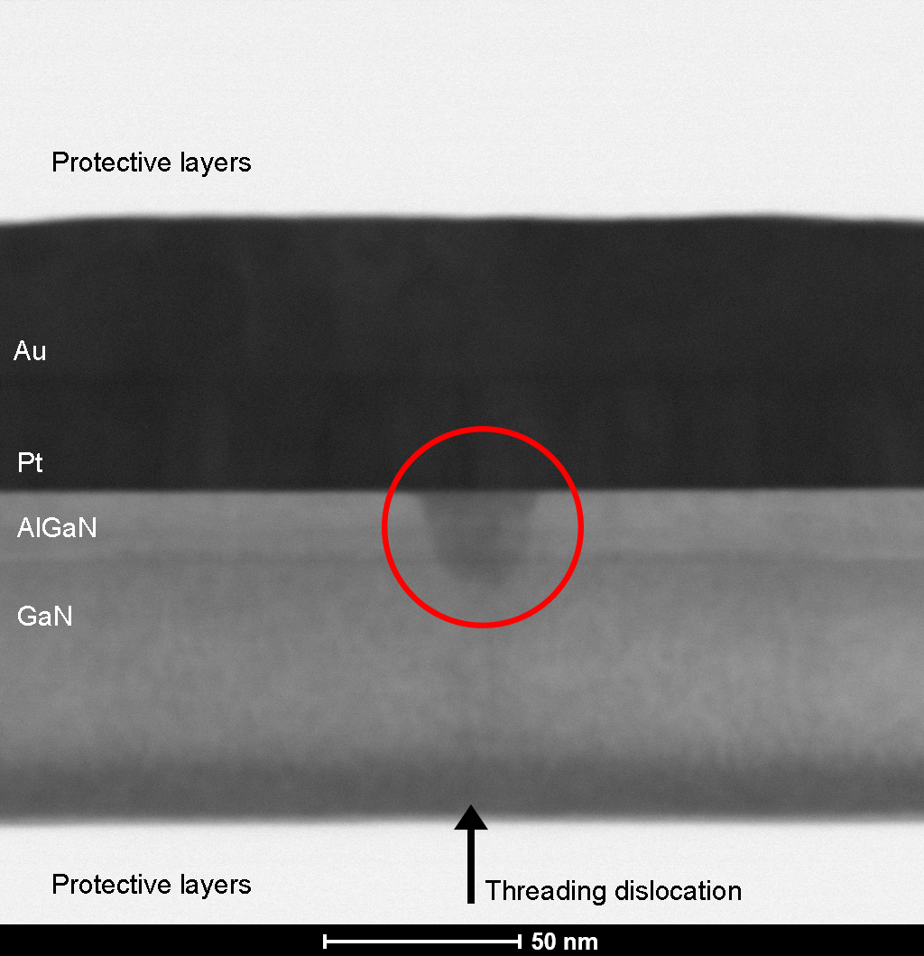
As part of the "iRel 4.0"-project, Fraunhofer IMWS has developed a new solution for approaching this problem. By combining different methods of sample preparation, the whole localized defect area is analyzed by transmission electron microscopy. In a first step, the entire defect area is scanned for nanometer-sized defects in a planar orientation. Additional cross-sectional samples are then taken from this sample to match the defects within the different layers and to be able to characterize them down to atomic resolution.
"As part of our collaboration with United Monolithic Semiconductors SAS and the University of Padua, we were, for the first time, able to identify metal-inclusions of 20 nanometers in size causing electrical short circuits. The defect structure could be analyzed in detail with the help of high-resolution transmission electron microscopy. This showed that the defects found are related to specific crystal defects in the epitaxially grown GaN layer and thus have a process-related root-cause," says Frank Altmann, Head of the Business Unit "Materials and Components for Electronics".
The objective of the European project "iRel 4.0" (Intelligent Reliability 4.0) is to improve the reliability of electronic components and systems by reducing the failure rate along the entire value chain. The aim is to double the service life of components, increase the learning curve by 30% by means of data analysis, detect defect formations earlier and reduce failure rates by 30%. The innovative approaches in quality assurance are intended to strengthen the competitiveness of the European semiconductor industry.
The project runs over a period of three and a half years and is financed by investments from industry, grants from the individual countries involved and the European "Joint Undertaking" ECSEL (Electronic Components and Systems for European Leadership).