 Fraunhofer Institute for Microstructure of Materials and Systems IMWS
Our Business Unit investigates components, systems and materials of electronics and microsystem engineering, for example integrated semiconductor circuits, sensors, electronic components and assemblies. We focus on complex failure diagnostics for field returns, tracking of causes of faults in qualification or in production and in in-depth understanding of the relationship between technological process and application conditions with microstructure and material properties as well as with the affected functional performance in detail.”
Services offered
Tabbed contents
Automotive Packaging
Failure analysis and material diagnostics for electronic systems
Factors triggering defects are identified and the corresponding failure mechanisms reconstructed. This is the base for increasing the reliability of electronic systems — after all, once we are aware of these defect causes, we can use this understanding to develop effective countermeasures and minimize the risk of failure.
Services:
- Comprehensive and time-efficient failure analyses for packaged components and integrated assemblies under one roof
- Material diagnostics and microstructure analyses of all materials and material combinations used Material characterization of new metallization systems and metal lines as well as encapsulation materials that are stable at high temperatures
- Material characterization and failure analysis of electronic packages (SiP, eWLB, PLP, MID, embedded components) and systems
- Extensive, time-efficient physical failure analysis workflows for packaged components and integrated assemblies from one source
- Modeling and simulation of the mechanical, thermal and thermos-mechanical properties of components
- Consultation on complex failure phenomena
- Analysis of material interaction for 2nd level reliability

Tailored test development

Rendering of the microstructural orientation of wire contacts measured by means of EBSD technique by a scanning electron microscope
The development of new testing methods tailored to the individual needs of our customers helps to lay the foundations for fast, efficient assessment of the material behavior under operational conditions.
Services:
- Mapping of the state of the art based on literature research
- Drawing up concepts for tailored test development
- Development of adapted tests and verification
- Development of methods for failure diagnosis and quality control
Material diagnostics Power electronics
Material diagnostics and failure analysis
We use material diagnostics methods to develop an in-depth understanding of materials under operational conditions and support our partners in the development of innovative material solutions and technologies for power electronics. We use our highly effective failure diagnostics and process-based expertise to support our partners by efficient failure diagnostics and process know how to assess damage cases and perform root cause analysis for product complaints. We provide various high-resolution analysis methods to conduct microstructure-based reliability analyses helping to secure long operational lifetimes.
Services:
- Microstructure diagnostics
- Mechanical testing and parameter identification
- Finite-Element-Analysis
- Failure localization and non-destructive analysis (SAM, X-ray, CT, lock-in thermography)
- Efficient site specific preparation of failures with nm precision (FIB, plasma FIB, ion etching, lasers, metallography)
- Microstructure and material diagnostics (SEM, EDX, WDX, EBSD)
- Nanoanalytics (TEM, TEM-EDX, AFM)
- Surface and trace analysis (XPS/ESCA, ToF-SIMS, ICP-MS)
- Polymer analytics (DSC, TGA, DMA)
- Comprehensive correlation of analysis results of the failure and defect modes/structure-property relationships
- Mechanical tests, modeling, simulation

3D X-ray analysis for process evaluation in the development and introduction of innovative new materials; in this case, a CT scan of a power electronics module with inorganic compound.
In addition, we support our partners with microstructural and micro-mechanical characterization for the development and qualification of new material solutions and manufacturing processes for industrial usage. With our wide range of state-of-the-art, optimized diagnostics methods, we also provide support to optimize production yields.
Optimization and development of test methods

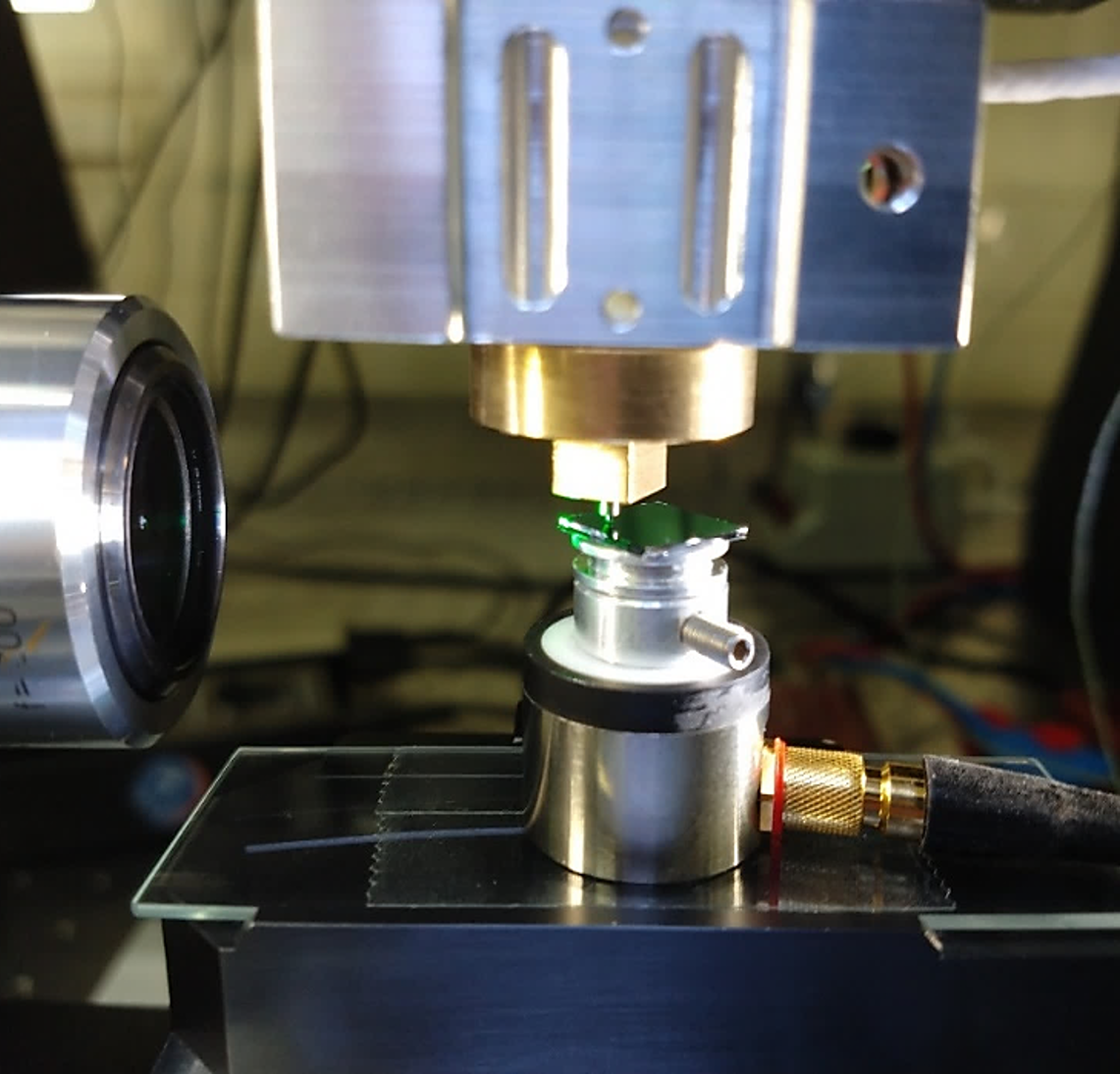
ML-based porosity analysis of silver sintering layers by means of acoustic waves
The development of new test methods adapted to the individual needs of our customers provides the basis for a fast and efficient evaluation of the respective material behaviour under operating conditions without over-testing.
Services:
- Mapping the state of the art on the basis of literature research and empirical values
- Creation of concepts for customised test development
- Development of adapted tests and verification
Micromechanical testing and simulation
Simulation and modeling
Finite-Element-Analysis (FEA) help us to better understand complex material interactions within materials and components. We provide support at the following areas.
Services:
- Mechanical, thermos-mechanical and multi-physical Finite-Element-Analysis
- Application of fracture mechanical, probabilistic and fatigue-based damage models, sub-modeling of failure modes
- Multi-physical process simulations
- Numerical design-, material- and process optimization
- Microstructural material design and failure analysis based on continuum mechanical approaches
- Model verification by experimental approaches, failure analysis and high-resolution material diagnostics

FEA of the stress generation on semiconductors through wire bonding
Test development for material characterization
Development of test structures for material characterization
The development of tailored test methods to the individual needs of our customers allows an enhanced material modeling related to operational conditions.
Services:
- Development of customer-specific tests related to material- and device characterization
- Test development taking material specific mechanisms into account
- Experimental verification of failure modes under customer-specific loading scenarios
- Support for the standardization of specific test methods
Material characterization
High-resolution hardness mapping of a molding compound with fillers
Material-specific and application-oriented material characterization is a base for sufficiently accurate simulation results. This requires customized experimental characterization approaches and specific parameter identification according for appropriate material laws.
Services:
- Application standardized or customer-specific tests for material characterization
- Identification of extended material parameters needed for FEA (non-linear, temperature-dependent, fracture mechanical, etc.)
- Local material characterization by means of nanoindentation in the sub-micrometer range (temperature dependent, mapping of modulus and hardness for heterogeneous materials)
- Characterization of thin films, functional layer and layer-stacks
- Estimation of parameters up to the high temperature range
Determination of parameters for failure and degradation models
Reliability assessment using FEA requires not only knowledge of suitable material parameters that facilitate the calculation of current load conditions, but also parameters for degradation and damage models. This, in turn, requires an in-depth experimental characterization of failure mechanisms.
Services:
- Identification of failure and degradation parameters
- Calculation of fracture mechanical parameters for bulk materials and interfaces
- Fracture mechanical characterization of bond strengths
- Probabilistic strength assessment of materials for process optimization and robustness validation
- Micromechanical determination of fatigue parameters (LCF and crack growth)
- Characterization of failure modes for thin layers (nano-scratch test, nano-wear)
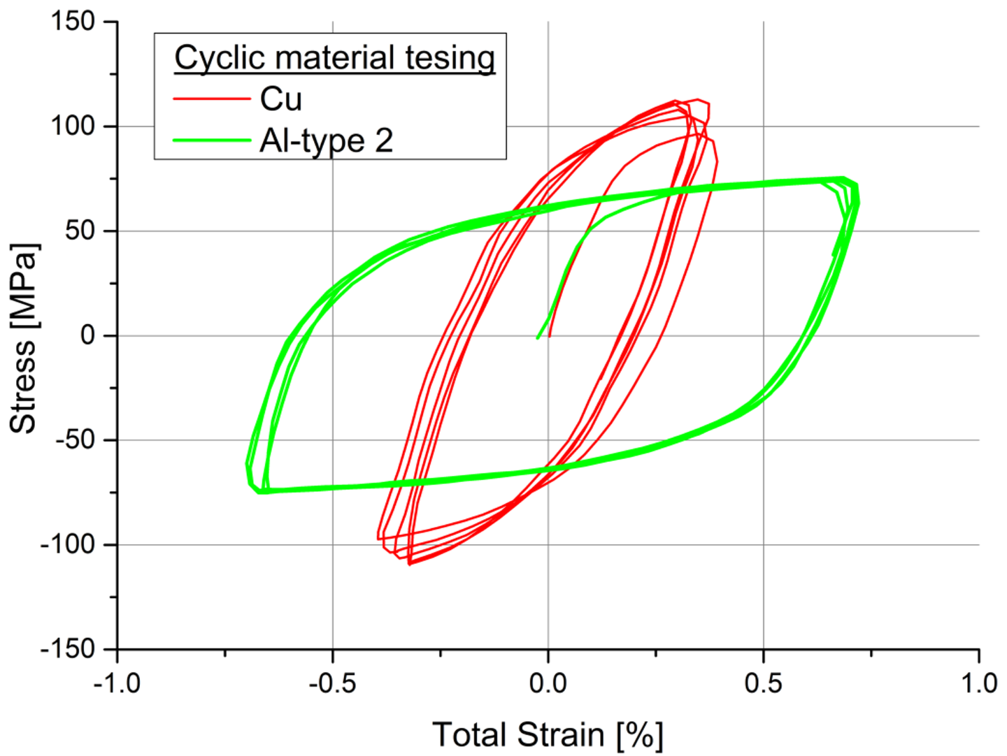
Cyclical testing of bond wire materials
Package and Assembly
Material and component characterization in the development phase
Material and component characterization tailored to the individual needs of our customers for fast, efficient assessment of the material behavior during the developmental stage.
Services:
- Analysis of the chemical composition
- Determination of mechanical/ electrical/ thermal material parameters
- Microstructural analysis
- Aging tests (degradation under defined loads)

Microstructure and grain structure analysis of bond wire material
Support to optimize production and processing
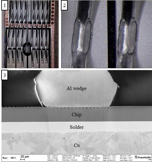
Characterization of the connection formed between the wire bond contact and semiconductor metallization
We help our customers to quickly and efficiently assess material behavior during production.
Services:
- Analysis of interconnect quality (mechanical/microstructural)
- Evaluation of the processability
- Reliability analysis of the interconnects
- Contamination analyses of the contact areas
Analysis of failure modes, degradation mechanisms and failure risks
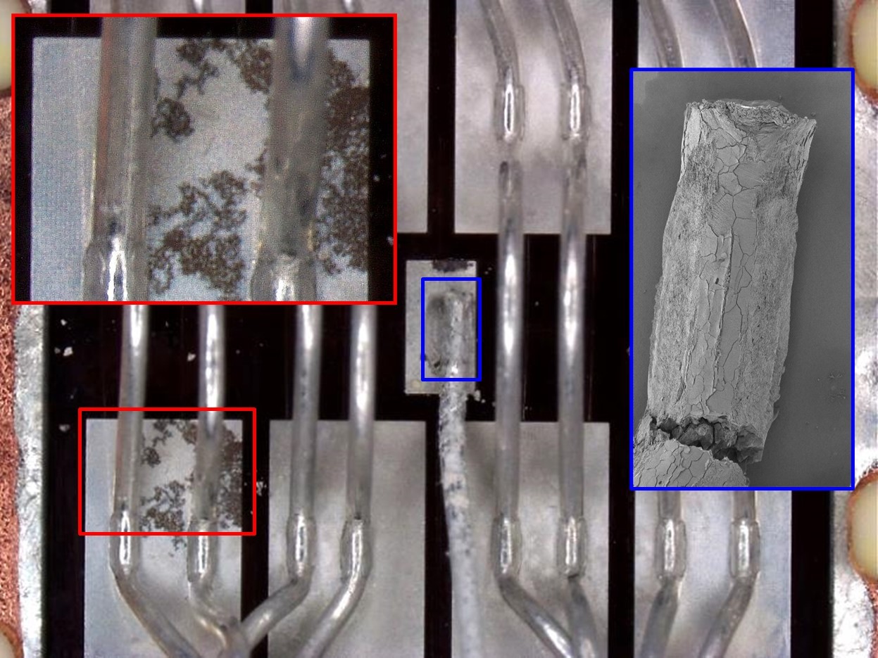
Dendrite formation on the semiconductor metallization as well as wire material embrittlement on a contaminated IGBT component
Factors triggering defects are identified and mechanisms that have led to failure are reconstructed. This way the reliability of electronic systems can be increased, effective protective measures developed, and the risk of failure minimized.
Services:
- Defect localization (visual/electrical/thermal/acoustic) and target preparation (laser/ion beam/metallographic/chemical) at the highest level
- Microstructure analysis down to the atomic dimension
- Chemical element analysis for all aspects (surface/volume/thin layers/particles)
- Clarification of the defect mechanism and derivation of counter-measures as well as estimation of further failure risks
Simulation and estimation of service life
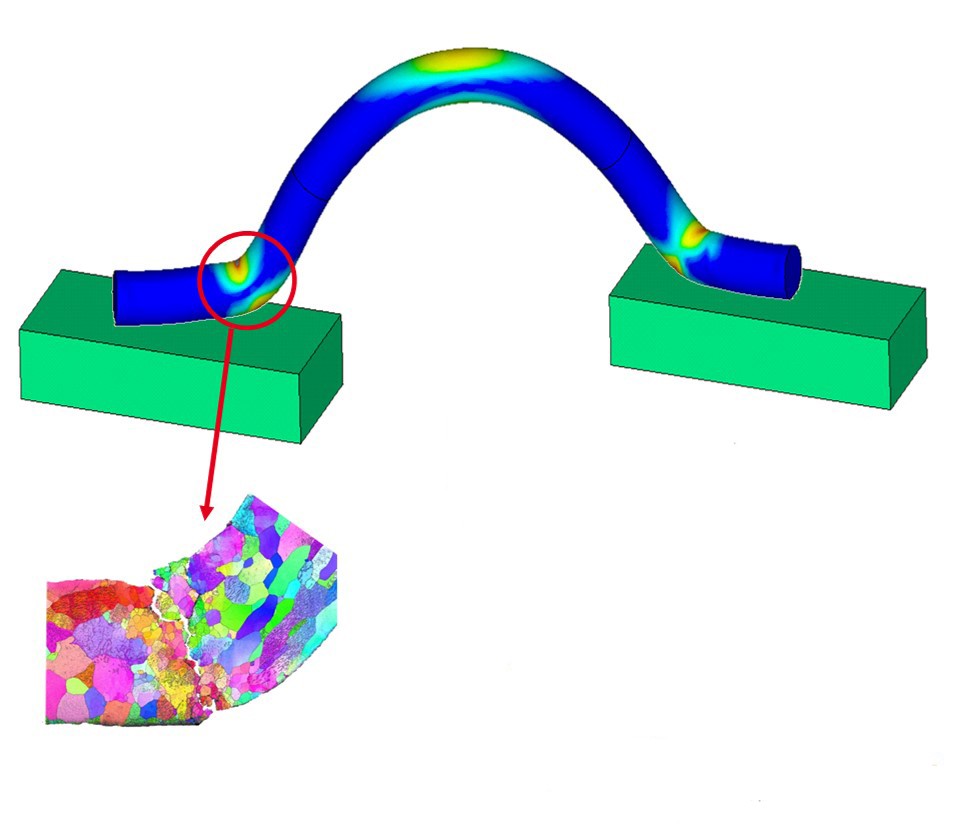
Grain structure representation of a degraded bond interconnect and recreation of the load scenario in the FE model to estimate the service life
FE simulations allow us to mathematically model the influences of material parameters, assembly conditions, process parameters and load scenarios to optimize material, process and structural designs, estimate service life spans and replicate failure mechanisms.
Services:
- Simulation of specific load cases (mechanical/thermal/electrical) for degradation and service life estimation
- Simulation to accompany component development (material selection/contact geometry/processability)
- Inverse simulation for verification of defect mechanisms and estimating the effectiveness of corrective measures and counter-measures
Development of tailored test and analysis methods
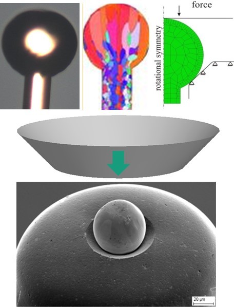
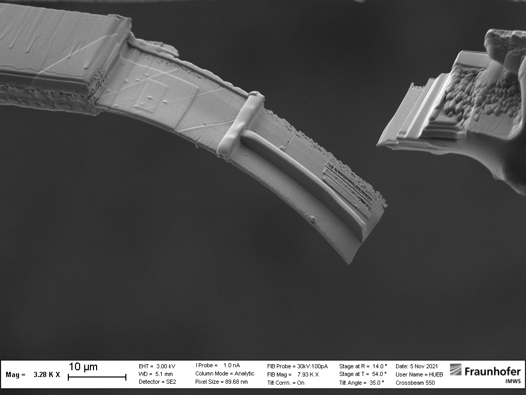
Structure-property correlation on a free air ball by means of capillary pressure test
Further and new developments of component and system technologies require continuous assessment, adaptation and the new development of test, preparation, and analysis methods, including verification and definition of assessment criteria. Our wide-ranging portfolio of material, process and application expertise combined with our test and analysis knowledge as well as our cooperation with systems and device manufacturers are the basis for our contributions in that field.
Services:
- Modification as well as new or further development of test and analysis methods/devices (including assessment criteria) in accordance with individual requirements
- Verification of the validity of existing test and analysis methods/devices as well as the associated assessment criteria
Physical failure analysis
Localization of electrical defects
In order to identify local defects in integrated circuits, we use optical, thermal and electron beam-based failure diagnosis techniques. Integrated circuits with electrical malfunctions such as short circuits, high-resistance or open contacts or discrepancies in power consumption and functionality are examined and corresponding defects are localized together with the customer.
Services:
- Measurement of characteristics at device and single transistor level by means of local probing under a light microscope or within a scanning electron microscope (SEM nanoprobing)
- CMP delayering of integrated circuit structures to access at transistor level for nanoprobing
- SEM-based potential contrast and current mapping techniques (EBIC, EBAC, EBIV, e-beam probing)
- High-resolution lock-in thermography to localize thermally active defects
- Emission microscopy to localize electrical active defects
- Circuit edit and preparation of local contact pads by means of focused ion beam technique (FIB-CE)

Process characterization and failure diagnostics
High-resolution microstructural analysis is used to verify geometrical process deviations and contaminations and to derive suitable optimization approaches and corrective actions. Target preparation methods and physical analyses are used to localize electrical defects, to determine failure root causes and degradation mechanisms which led to electrical mail functions within the device. In complex failure scenarios we evaluate operating conditions and failure histories together with the client, draw up corresponding anamnesis and derive analysis strategies, which allow us to identify the causes triggering the failure and take corrective actions.
Services:
- FIB/REM sampling of localized defects to find nm defects
- FIB target preparation of IC structures and defects
- High-resolution electron microscopic analysis by means of scanning electron microscopy and atomic resolved transmission electron microscopy including element verification by means of EDX/EELS
- Surface and trace analysis by means of ToF-SIMS and XPS to identify impurities in IC interfaces and on contact surfaces
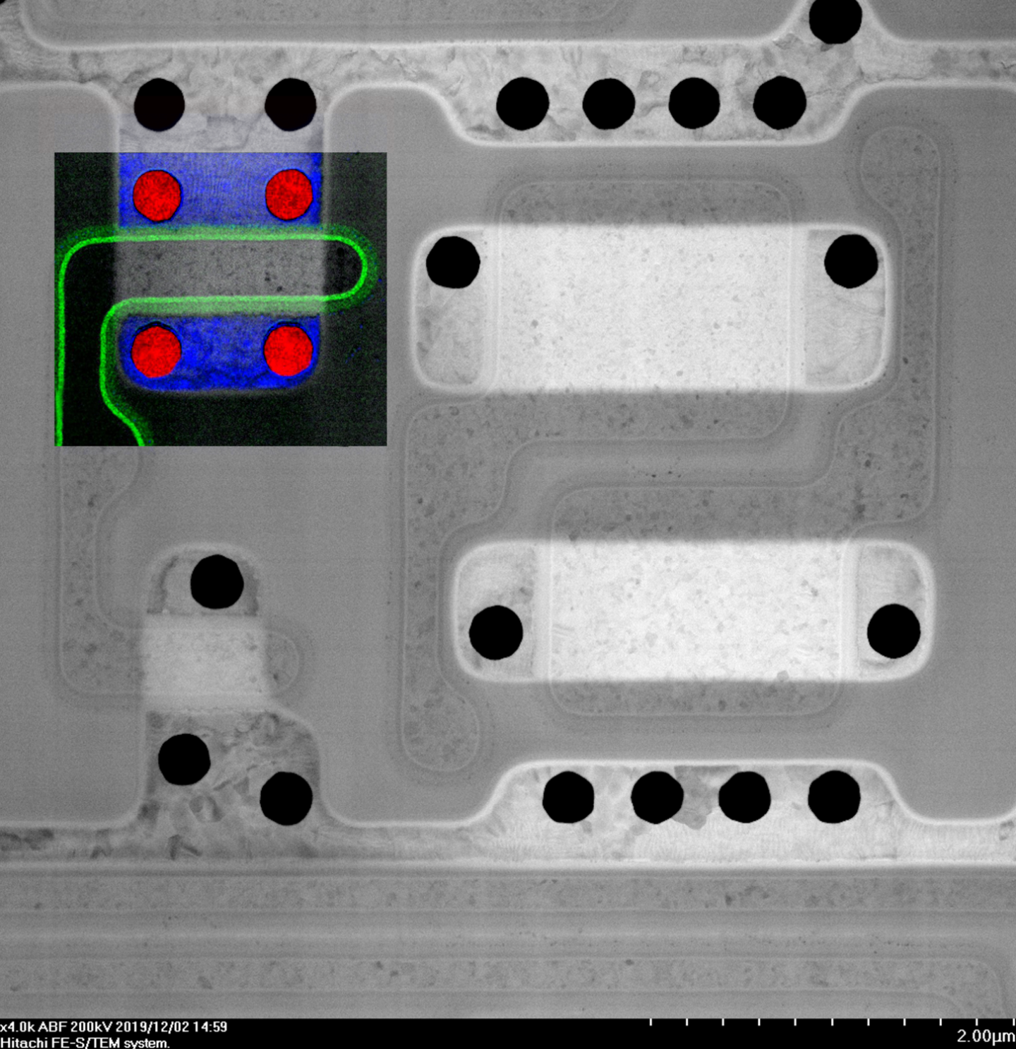
STEM-ABF imaging and local EDX mapping of a CMOS inverter in planar direction with nitrogen (green), cobalt (blue) and tungsten (red) in PMOS
Development of analysis techniques
For the localization and failure diagnostics of electrical defects, corresponding analysis methods are adapted and further developed to meet the respective requirements for new technologies and component designs. The aim is to increase the detection sensitivity and spatial resolution for defect localization and to improve the FIB target preparation methods in terms of precision and minimal artefacts for advanced IC technologies with lower feature sizes.
Services:
- Further development of SEM in-situ nanoprobing techniques and corresponding preparation methods
- Electron beam-based mapping techniques for localizing electrical defects inIC structures
- Laser and plasma FIB preparation of extensive cross-sections and coupled Ga-FIB target preparation
- FIB trenching for backside access for FIB-CE and E-Beam probing
- Repackaging (rebuilt of defective components in new test environments)

Focused ion beam lab
Non-destructive defect localization
Development and application-specific design of focused acoustic transducers
Sensitivity and image resolution are key criterias for non-destructive acoustic imaging. However, due to the materials found between the transducer and test region in non-destructive inspections, these two parameters can be severely impacted. The solution here is offered by an ultrasound transducer which is optimally tailored to the sample in terms of frequency and focus and which ensures the best possible performance during ultrasound-based defect localization.
Services:
- Simulation of the transient sound propagation from the piezo element through to the sample (and back)
- Design and dimensioning of the focusing aperture
- Development and manufacturing of application-optimized transducer together with expert partners
- Specific acoustic microscopy applications

SAM wafer inspection
Development of measurement technology and setups for acoustics and thermography
In defect analysis, the physical root causes are of key importance. Failures are localized at macroscopic and microscopic level to be able to subsequently apply corresponding high-resolution analysis techniques. The original sample state must be maintained, so as not to change the defect scenario. Depending on the type of defect (mechanical or structural changes, delamination, electrical short circuit/open circuit, etc.), various contrast mechanisms may be useful. We adapt our measurement techniques to the customer-specific requirements and evaluate the applicability on different types of devices and defects for the purposes of failure analysis and quality assurance.
Services:
- Design, development and evaluation of non-destructive, working metrology in the areas of acoustics (ultrasound), thermography and magnetic field sensors
- Evaluation of lock-in thermography, acoustic microscopy and magnetic field microscopy for questions regarding non-destructive defect localization
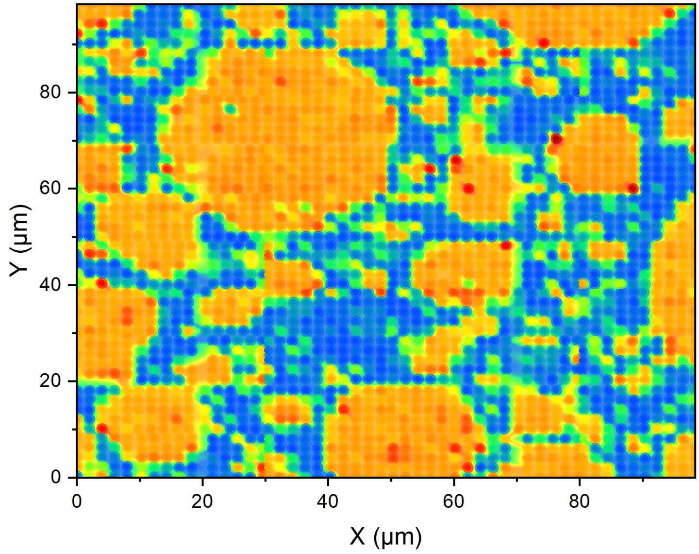
Deep learning assisted quantitative assessment of the porosity in Ag-sinter joints based on non-destructive acoustic inspection
Software implementation of the hardware

ToF-SIMS sample holder with inserted sample
The data acquired with the developed measurement technique is usually in form of time- signal-based data sets or image stacks and typically has a complex structure and is of considerable scope. In order to manage the measurement technique and handle the data, the hardware for a developed measurement set-up must be implemented through the installation of software. This includes both communication with the hardware and the control thereof, as well as the time-critical handling of the incoming data.
Services:
- Software-side implementation to establish communication with the hardware for device control
- Software implementation for managing data acquisition and time-critical handling of data
Development of signal and data analysis methods including software
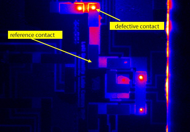
Localization of high-resistance flip chip contacts through an SI layer
The processing of data for analysis purposes is part of the workflow. Our team develops methods for signal analysis based on the issue in question so that the information relevant to the issue can be extracted. In particular, methods for machine learning based data analysis — specifically deep learning — are also used to increase the reliability of interpretation and thereby the reliability of the entire analysis. The developed algorithms are combined in user software.
Services:
- Algorithms and method development of standard signal analytics
- Development of analysis concepts based on machine learning
- Implementation in user software
GaN-HEMT devices
Process and technology characterization
High-resolution analysis methods are used to examine GaN-epi layer systems and GaN-HEMT structures to measure layer thicknesses and residual stresses, determine defect densities and identify surface and interface contaminations. To this end, we support our partners in the development and optimization of GaN-epi processes and functional HEMT structures on different substrates.
Services:
- High-resolution, electron microscopic analysis of the GaN-epi layer structures and crystal defects by means of (S)TEM/EDX
- Analysis of the lattice mismatch and residual stresses in GaN-epi layers by means of electron beam diffraction (NBED)
- Verification of process-related impurities on substrate surfaces and in layer interfaces with gate and ohmic metal contacts and passivation
- Verification and qualification of doping in p-GaN by means of spatial-resolution trace analysis (ToF-SIMS)

Residual strain analysis of GaN-epi layers on silicon by means of NBED experiments and correlated XRD reference measurements
Failure diagnostics and clarification of failure mechanisms
Pitting defect on the Schottky gate of a GaN-HEMT
We specifically examine stressed and failed GaN-HEMT devices in order to determine new, technology-specific failure modes, root causes of failures and degradation mechanisms. The aim is to identify design or process-related weaknesses in the GaN-HEMT structures and to support further technology developments.
Services:
- Localization of electrically active defect structures in GaN-HEMT structures by means of electroluminescence microscopy and high-resolution lock-in thermography
- Localization of critical defects in the GaN-epi by means of electron beam-based current mapping (SEM-EBIC)
- Precise target preparation of defects using a focused ion beam technique and analysis of defect structures by means of atomic resolution analytical electron microscopy to identify and clarify the root causes of stress and application-related degradation mechanisms
Further development of analysis methods
For the verification of defect mechanisms and failure modes in GaN-epi and GaN-HEMT structures, we are continually improving our analysis methods for the precise localization of electrically active defects, for target preparation and high-resolution structure analysis.
Services:
- Front and -back side localization and identification of electrically active defects by means of electroluminescence spectroscopy and lock-in thermography
- Electron beam-based techniques for the visualization of p-n junctions and defect identification within the GaN-epi (EBAC, EBIC, ECCI)
- High-resolution mapping of crystal lattice parameters and corresponding deviations by means of nanobeam electron diffraction (NBED) in the STEM
- High-resolution ToF-SIMS analysis for the detection and quantification of dopant elements and hydrogen in GaN-EPI structures
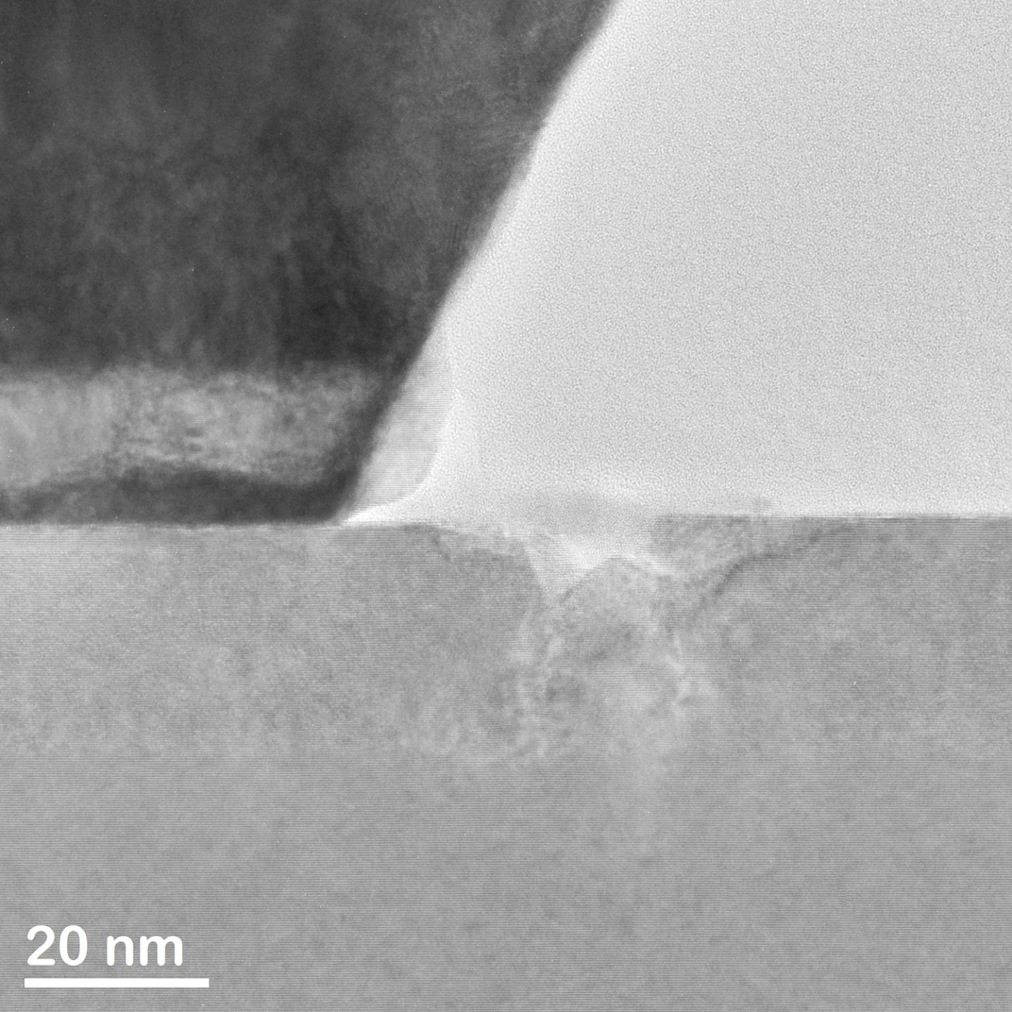
FIB-prepared TEM lamella for the combined cross-section and planar analysis of defect sites