Physical failure analysis

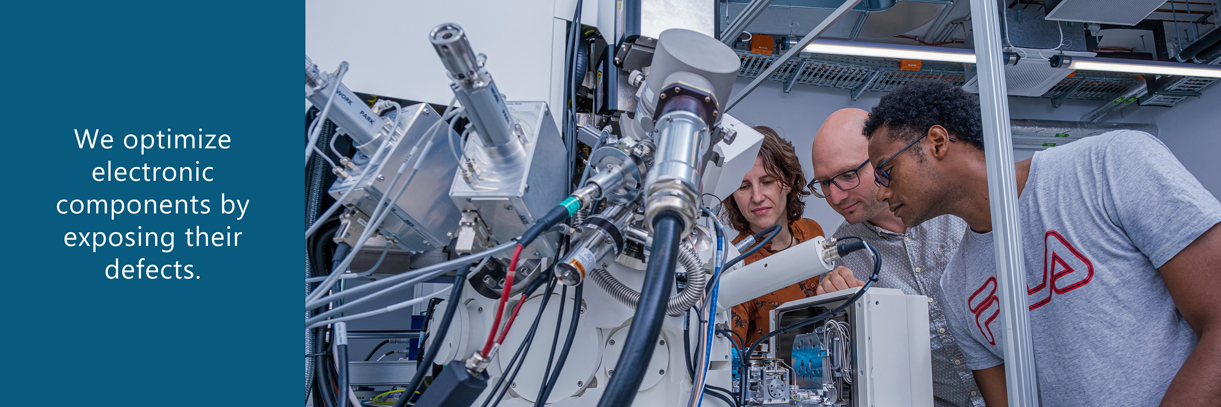
Quality assurance and structural analysis for semiconductor components

Integrated circuits on silicon substrates are used today in almost every electronic device we come across in our everyday lives. Future technologies such as autonomous driving, electromobility or the internet of things require increasingly powerful and complex electronic components and systems. In addition to progressive miniaturization and the associated increase in performance and cost efficiency, the increase in robustness, especially for critical applications, also play an important role.

The constantly growing complexity of systems and the increasing demands on service life and reliability pose new challenges for quality assurance and the structural analysis necessary for it.


We offer our clients a customized analysis process

© Fraunhofer IMWS
TEM image of a transistor structure with electrically active crystal defects

We offer our customers a complete fault analysis chain - from sample preparation to structural analysis, chemical and electrical characterization and simulation. We focus on the needs of our customers and their active involvement in the analysis process by means of appropriate defect anamnesis and clarification of the previous defect history on the basis of existing analysis results.

What you can expect: a demand-oriented defect analysis

We support and accompany our partners:

  • with our in-depth expertise in the area of silicon technology
  • in the selection of the right methodology for targeted failure analysis
  • in the complex material and defect characterization of electronic components from the application areas automotive, RF and power electronics
  • in the development of preparation methods based on focused ion beams (FIB)
  • by quickly and purposefully addressing their problems

Your benefit: more reliable and robust products

We increase the reliability and robustness of products, thereby improving cost efficiency and supporting our customers in optimizing application-oriented manufacturing processes.

Services offered


Localization of electrical defects


Process characterization and failure diagnostics


Development of analysis techniques

Publications

Year Title/Author
2023

Backside Analysis Strategy to Identify a Package Related Failure Mode at an Automotive Magnetic Sensor Device 

M. Simon-Najasek; F. Naumann; S. Huebner; M. Lejoyeux; F. Altmann; A. Lindner

2022

Flyer: Physical failure analysis

2021

Local metal segregation as root cause for electrical shorts in highly doped pressure sensor devices

Simon-Najasek, M.; Diehle, P.; Große, C.; Hübner, S.; Brokmann, G.; Sprenger, B.; Sprenger, B.; Altmann, F.
2020

On-Wafer Fast Evaluation of Failure Mechanism of 0.25-mm AlGaN/GaN HEMTs: Evidence of Sidewall Indiffusion

Rzin, M.; Meneghini, M.; Rampazzo, F.; Zhan, V.G.; Marcon, D.; Grünenpütt, J.; Jung, H.; Lambert, B.; Riepe, K.; Blanck, H.; Graff, A.; Altmann, F.; Simon-Najasek, M.; Poppitz, D.; Meneghesso, G.; Zanoni, E.
2019

Non-invasive soft breakdown localisation in low k dielectrics using photon emission microscopy and thermal laser stimulation

Herfurth, N.; Wu, C.; Beyreuther, A.; Nakamura, T.; Wolf, I. de; Simon-Najasek, M.; Altmann, F.; Croes, K.; Boit, C.
2019

Adaptive low-temperature covalent bonding of III-nitride thin films by extremely thin water interlayers

Gerrer, Thomas; Graff, Andreas; Simon-Najasek, Michél; Czap, Heiko; Maier, Thomas; Benkhelifa, Fouad; Müller, Stefan; Nebel, Christoph E.; Waltereit, Patrick; Quay, Rüdiger; Cimalla, Volker
2017

High resolution physical analysis of ohmic contact formation at GaN-HEMT devices

Graff, A.; Simon-Najasek, M.; Altmann, F.; Kuzmik, J.; Gregusová, D.; Hascík, S.; Jung, H.; Baur, T.; Grünenpütt, J.; Blanck, H.
2016

Novel failure mode of chip corrosion at automotive HALL sensor devices under multiple stress conditions

Simon-Najasek, M.; Lorenz, G.; Lindner, A.; Altmann, F.